Decapsulating the component chemically to directly analyze the chip’s surface
Applied Standards
- MIL-STD-883 Method 2010
- MIL-STD-883 Method 2013
- AS6081
- IDEA-STD-1010
- ESCC 25300
Areas of application:
- Ascertaining overloading ( regarding ESD, EOS)
- Ascertaining the manufacturer (regarding originiality)
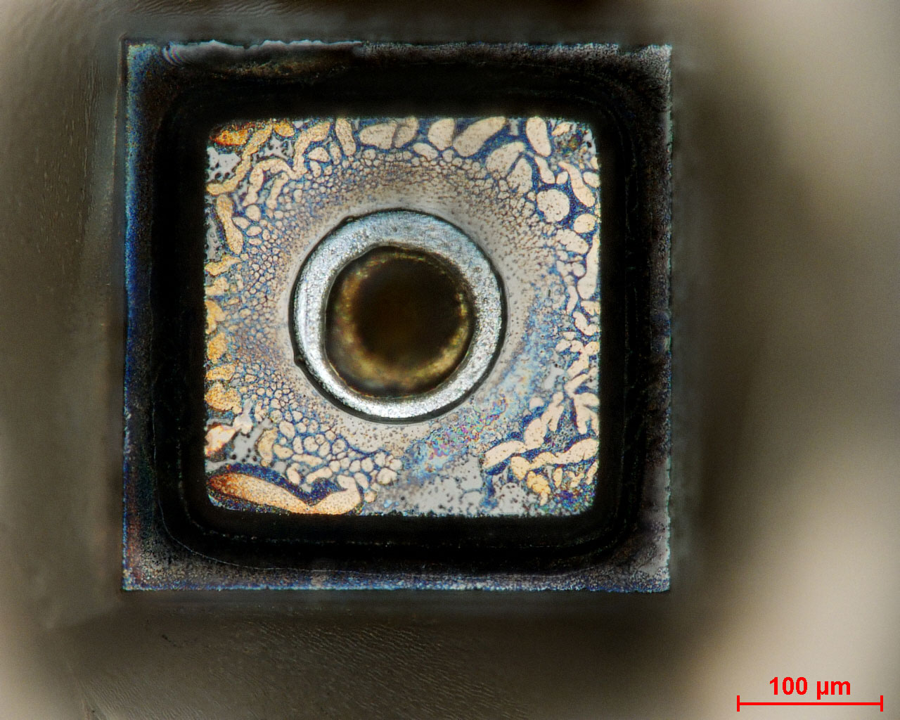
- Analyzing bonding areas, micro fractures, structural flaws
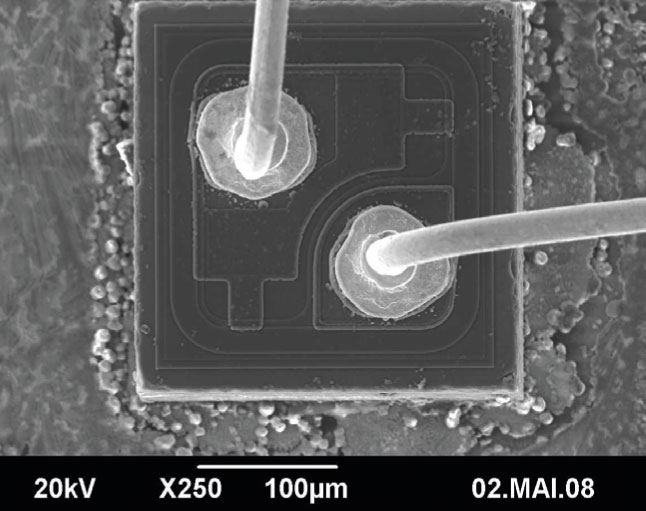
- Bond, pull and shear tests
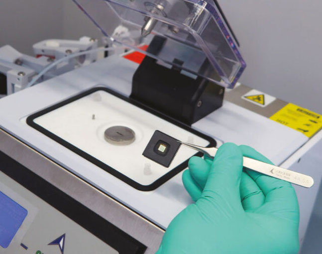
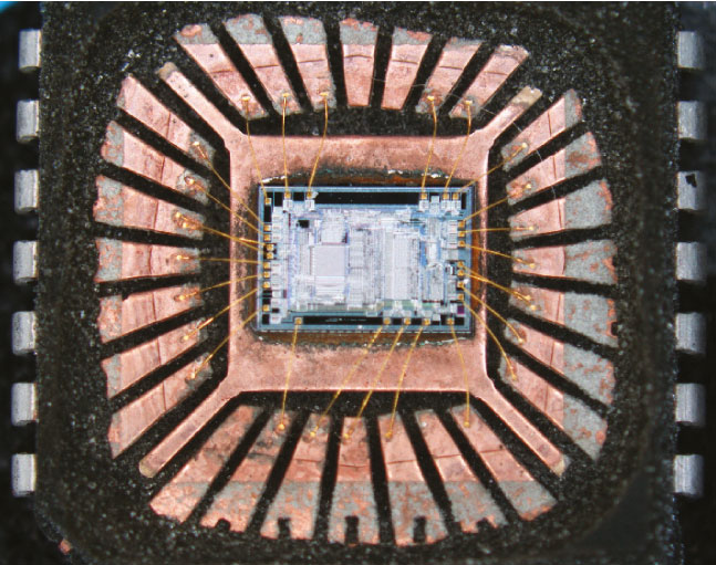
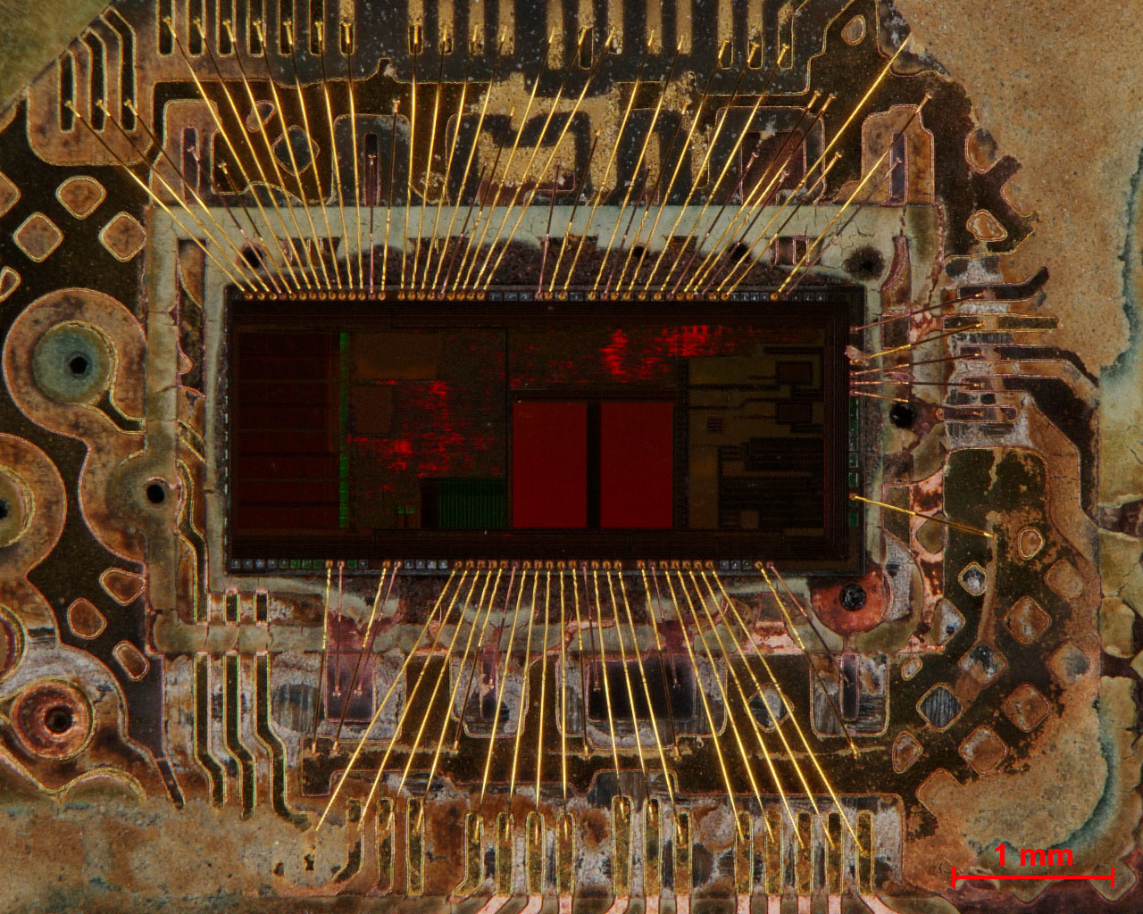
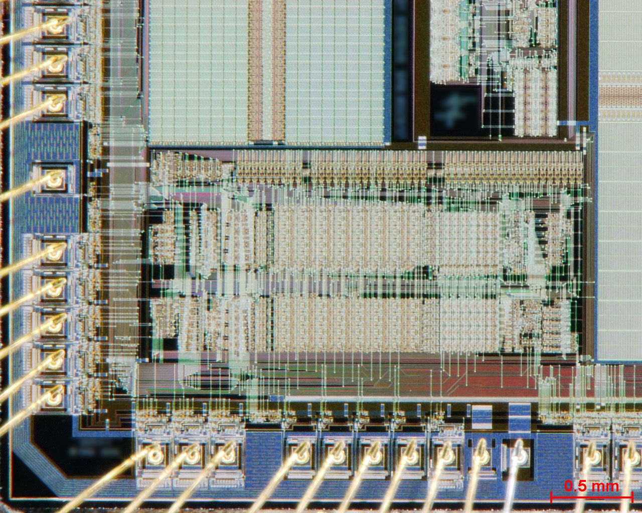
The chemical decapsulation of electronic components is of vital importance whenever it becomes necessary to directly analyze a chip’s surface, i.e., to ascertain the actual version of the chip in question or its manufacturer. HTV’s own, in-house developed, partly automated decapsulation process was developed in accordance with state of the art industry standards and can be adapted precisely to any component capsulation material to avoid internal damages.
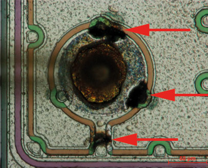
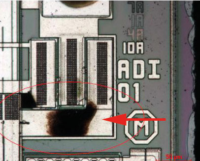
Eventual functional impairments, stemming from such strains of the component as ESD or EOS events, mechanical tension or similar effects, may be ascertained by analyzing the chip’s surface with light microscopy or scanning electron microscopy after the decapsulation.
Precise pull and shear testing devices make it possible to quickly ascertain bonding quality.
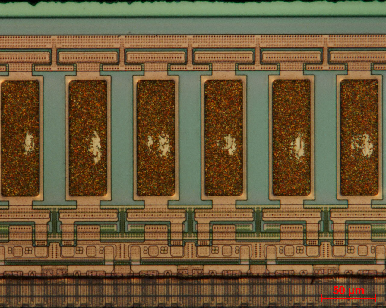
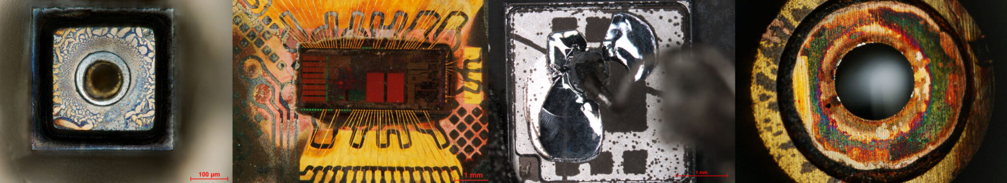
Electronic component damage examples