Analysis of data safety in electronic flash memories (e.g. NAND and NOR)
Applied standards
- JESD47
Memory qualification process:
- Aging of single memory areas or blocks with different numbers of erasure and writing cycles
- Writing of test data into the aged memory areas
- High temperature storage of the components to accelerate the discharge of electrons from the memory cells, e.g., for 100 hours at 125°C
- Reading the memory and analyzing the appearing bit tippers (Tolerant Verify)
- Graphical evaluation and report
Globally used electronics are changing heavily, which also specifically concerns memory components. Current developments in digital memory components are aiming to raise the speed and data transfer rate, reduce the power consumption, while at the same time raising the amount of written data per area unit more and more.
This trend however brings with it the complication that less and less electrons in a memory cell embody an information or a bit (0 or 1). Writing/programming and erasing a memory cell additionally damages its oxide or isolation layer/sheen? cumulatively.
with erased floating gate (condition: 1)
with written floating gate (condition: 0)
Given the ever increasing number of write and erase cycles, more and more electrons are discharged over time from the memory area of a memory cell, also known as a ‘floating gate’. Once this number of electrons inside a memory cell hits a certain threshold, the bit errs or tips over and the digital information becomes flawed. And once these bit errors inside a cell’s area have reached a certain number, the memory can no longer compensate with its own internal EEC (Error Checking and Correction).
High temperature storage to simulate accelerated aging can be done at the memories’ permissible maximum storage temperature (i.e., 150°C) or in accordance with specified norms of endurance testing (i.e., JEDEC STANDARD JESD47).
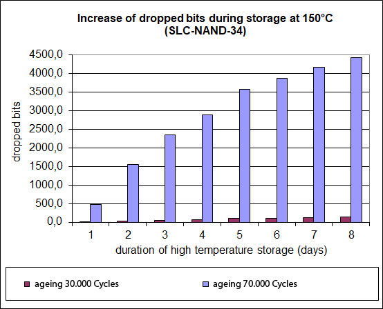
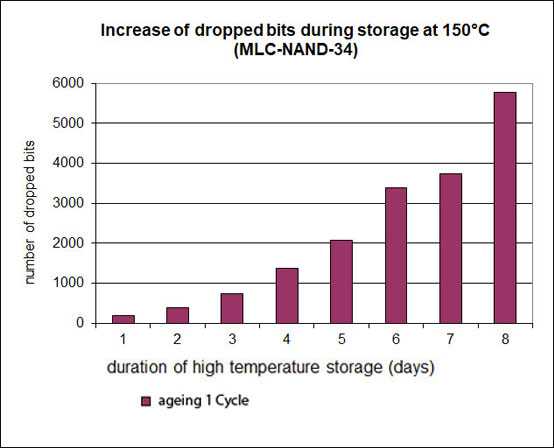
Knowledge of the quality or the service life cycle of the memory technology employed is of vital importance for its later application to ensure a smooth operation across the product’s entire service life. A memory cell’s endurance is defined as its maximum of write/erase cycles, in which it can retain the written data for a predetermined minimum amount of time without a power supply.
An HTV memory qualification can determine the quality of many different memory technologies, which in turn allows one to choose the most fitting technology for the corresponding application to ensure a sufficient amount of data retention for the entire service of the respective assembly.