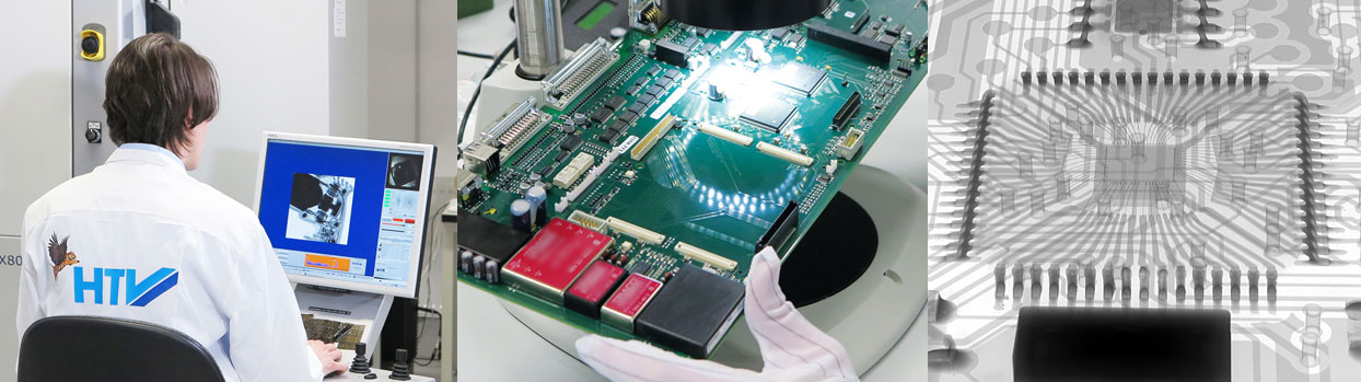
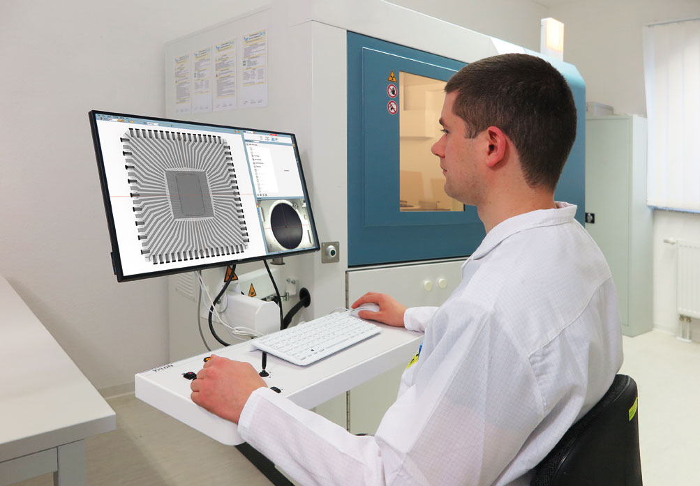
X-ray inspection to non-invasively analyze components and assemblies
Applied Standards
- DIN EN 61191-6
- MIL-STD-883 Method 2012
- AS6081
- IDEA-STD-1010
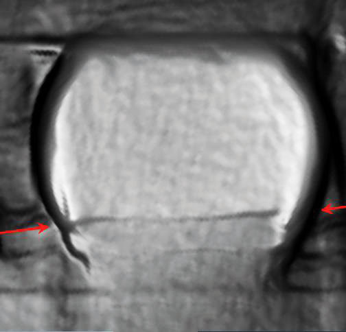
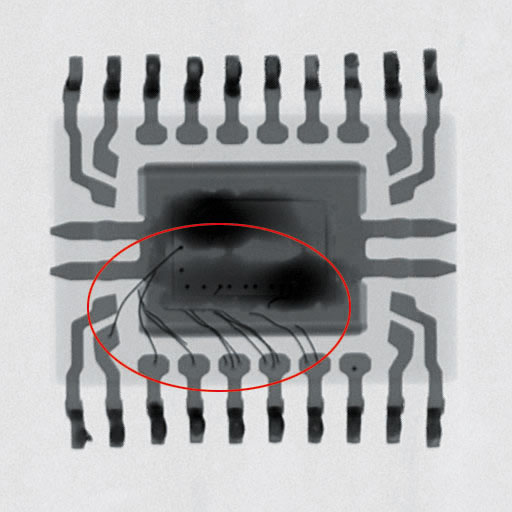
The necessity to non-invasively analyze components and assemblies very often demands an inspection via x-ray technology. With this, the lead frame, bonding wires and the chip’s position inside the component can be analyzed, as well as printed circuit boards in regards to their inner conductive lines.
In the case of components of rather dubious origin an x-ray inspection can reveal whethere there is a chip inside the component at all, if the manufacturer kept the required bond sequence, or if there are improper bond wire junctions.
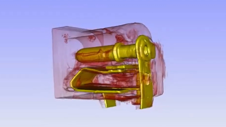
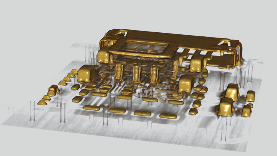
Areas of application – 3D X-ray / computer tomography (CT):
- Color-based highlighting of different materials to locate and analyze material and processing defects in components and assemblies
- Analyzing bond areas and lead frames (3D model)
- Ascertaining the contact area of spring-loaded press-in pins
- Analyzing crimp contacts
- Analyzing moulded components, i.e., wire connections inside transformers
- Determining sectional image planes for more in-depth analysis sample preparation, i.e., microsectioning
Printed circuit boards and crimp contacts in 3D X-ray
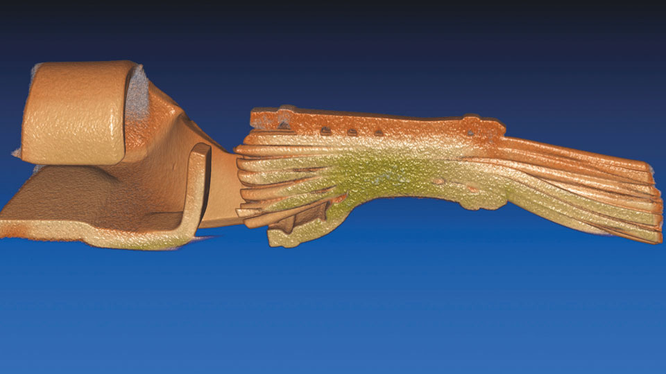
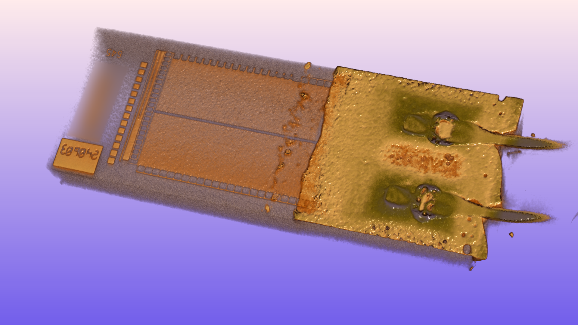
3D x-ray images using computed tomography (CT) for a very three-dimensional representation of hidden details enable an additional option to analyze components and assemblies in regards to possible material or processing defects with color-based highlighting, localization and investigation of different materials.
You are currently viewing a placeholder content from YouTube. To access the actual content, click the button below. Please note that doing so will share data with third-party providers.
More InformationAreas of application – 2D X-ray:
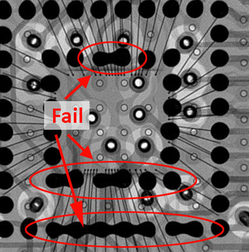
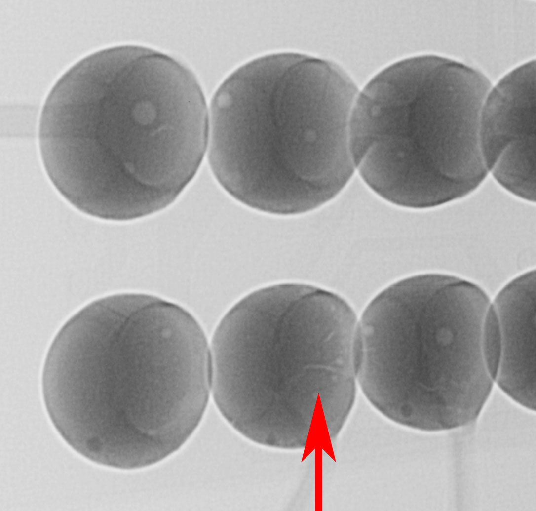
- Inspection of hidden solder joints (i.e., BGA inspection of the solder ball shape a check for possible void formation)
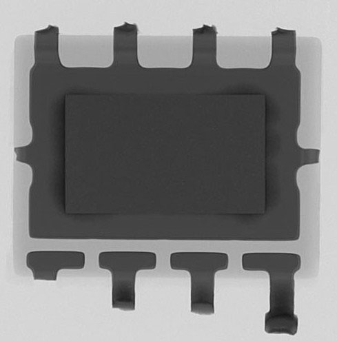
- Analysis of bonding areas and leadframes (i.e., looking for broken bonds)
- Analysis of contacts and solder joints (i.e., looking for anomalies or fracture formations)
- Analysis of the bond wires and the chip’s position inside the component
- Analysis of BGAs (i.e., looking for fractures and voids)
- Analysis of a chip’s silver conductive bonding to the leadframe (i.e., looking for voids)
- Analysis of the printed circuit boards plated through holes regarding CAF (Conductive Anodic Filament)
- Analysis regarding ESD and EOS damages
Electronic component damage examples
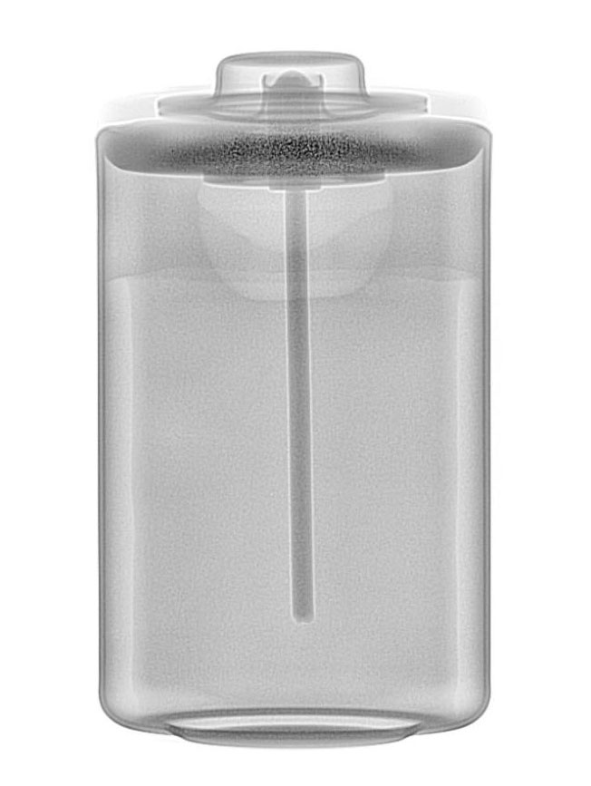
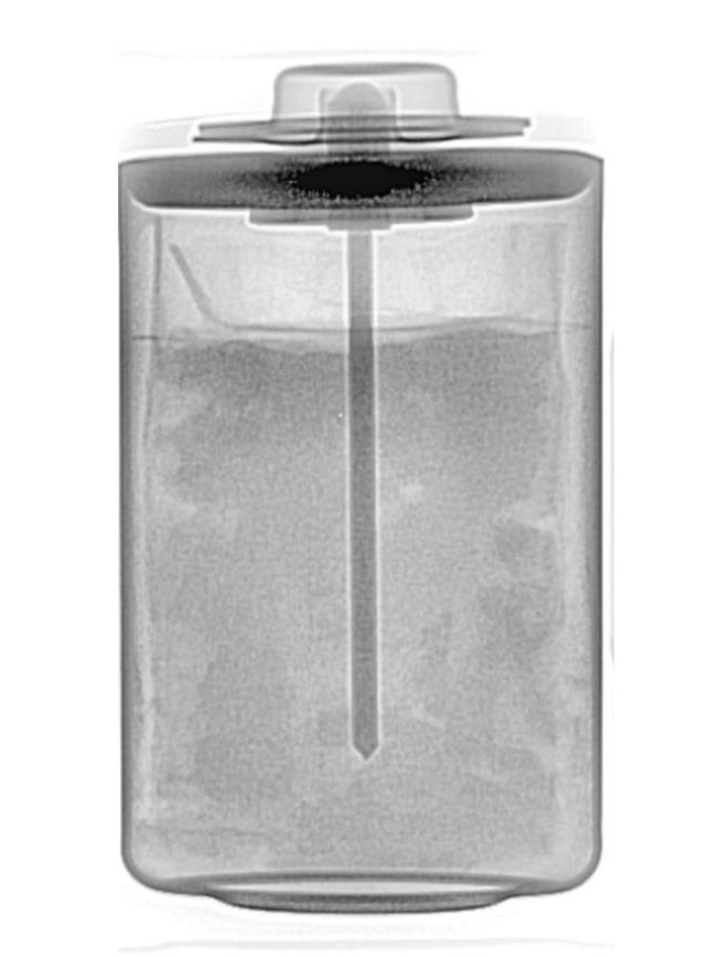
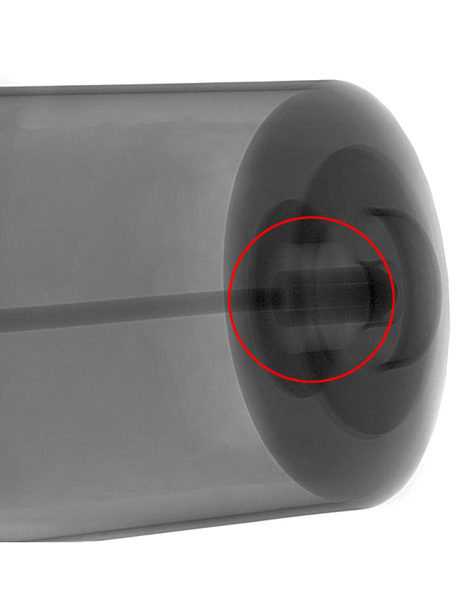
Battery damage examples
Li-ion batteries have shown a rather unexpectedly rapid discharge and in some cases a polarity reversal. The x-ray analysis has made enormous differences in the inner structures between the sample parts and the golden sample visible.
No defects could be identified in the glass-metal-bonding. However, as glass can not be depicted satisfiyingly in an x-ray analysis, it is advised to further analyse the inner structures via scanning acoustic microscopy.