
Development, testing software (and procedures), packaging
Owing to close cooperation with numerous European semiconductor and ASIC manufacturers the HTV corporate group is able to provide full support throughout the entire development process in the field of application specific integrated circuits or ASICs, making them one of the largest European service providers in the realm of outsourced semiconductor assembly and test (OSAT).
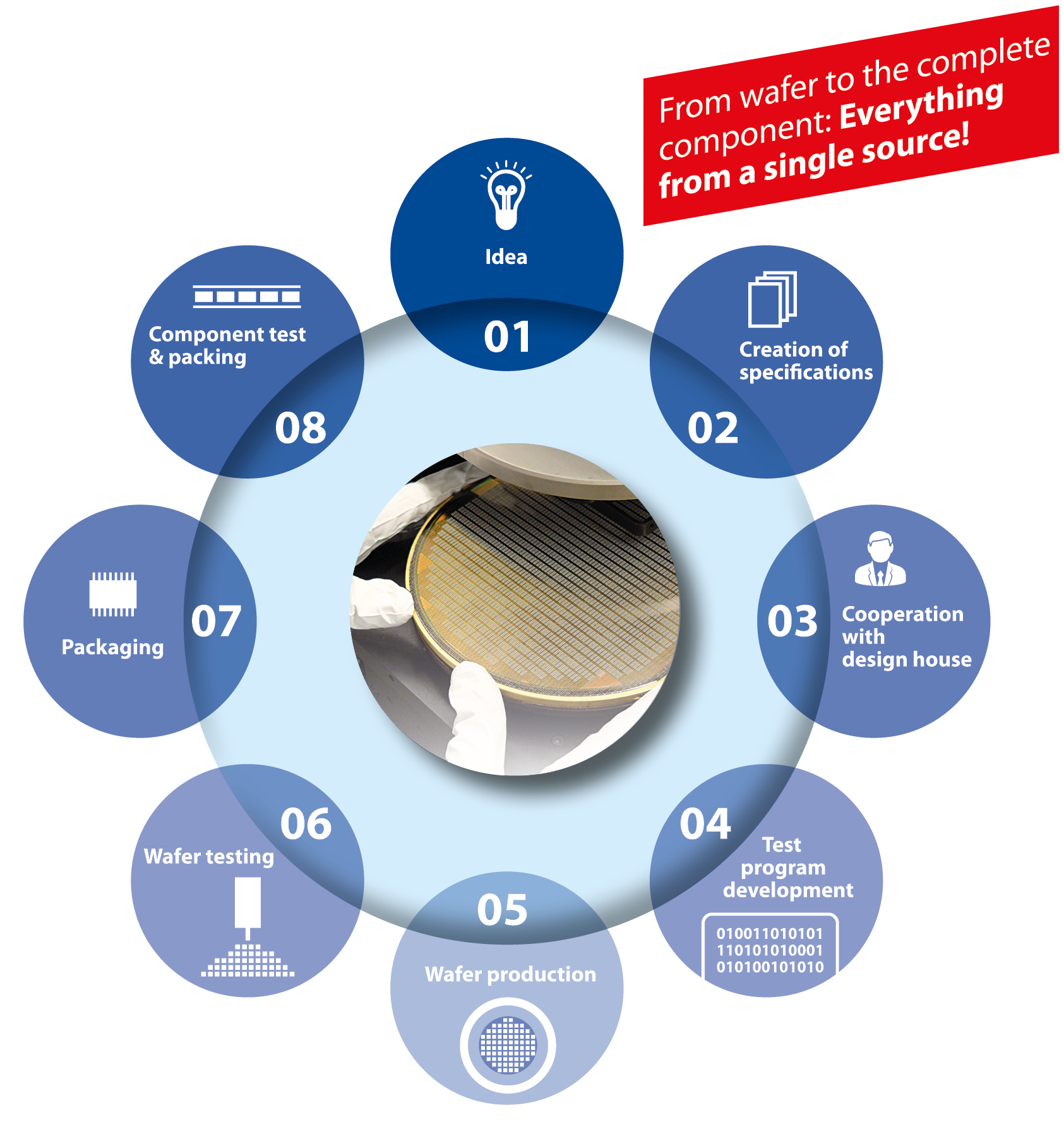
The customer’s idea and the specification creation
Once a customer has decided to employ an ASIC, maybe to replace several components on a circuit board to optimize that area, HTV provides support by first creating a tailor-made specification (e.g., application area, range of functions).
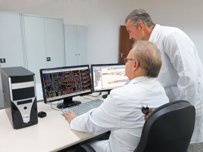
Cooperation with a design house and development of specified test programs
A spec document is drawn up in cooperation with a design house, in which the function (analog, digital, mixed signal) and the required parameters are defined. The design house then implements the document and designs the circuit and the actual ASIC layout. Meanwhile, HTV develops testing software specifically tailored to the datasheet and the function test.
Manufacturing and testing of wafers
Following the first part, wafers are produced in a foundry and tested on high-precision mixed-signal testing systems at HTV. If there are any deviations to be found in the first components manufactured in hardware (silicon), the ASIC layout is readjusted.
Component testing and assembly
A comprehensive final electrical test according to specified operating temperatures and individual requirements ensures the flawless functionality of the newly developed and housed component, if necessary. Subsequently the electronic components are measured and packaged into a blister reel through fully automatic taping and reeling systems.