Applied Standards
- DIN EN ISO 3497:2001-12
- AS6081
- IDEA-STD-1010
- EU-Richtlinie 2011/65/EU
- JEDEC JESD 213
Accreditations:
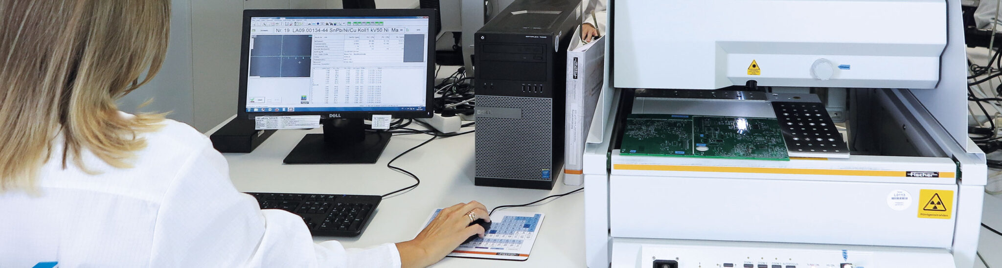
Accredited and globally acknowledged non-invasive layer thickness measuring to analyze metal coatings in the micrometer and nanometer range, such as:
- Solder surfaces of printed circuit boards
- Coatings of solder contacts or connectors
- Corrosion protection coatings
- Chromate coatings
- Finishes (i.e., the gilding of jewellery)
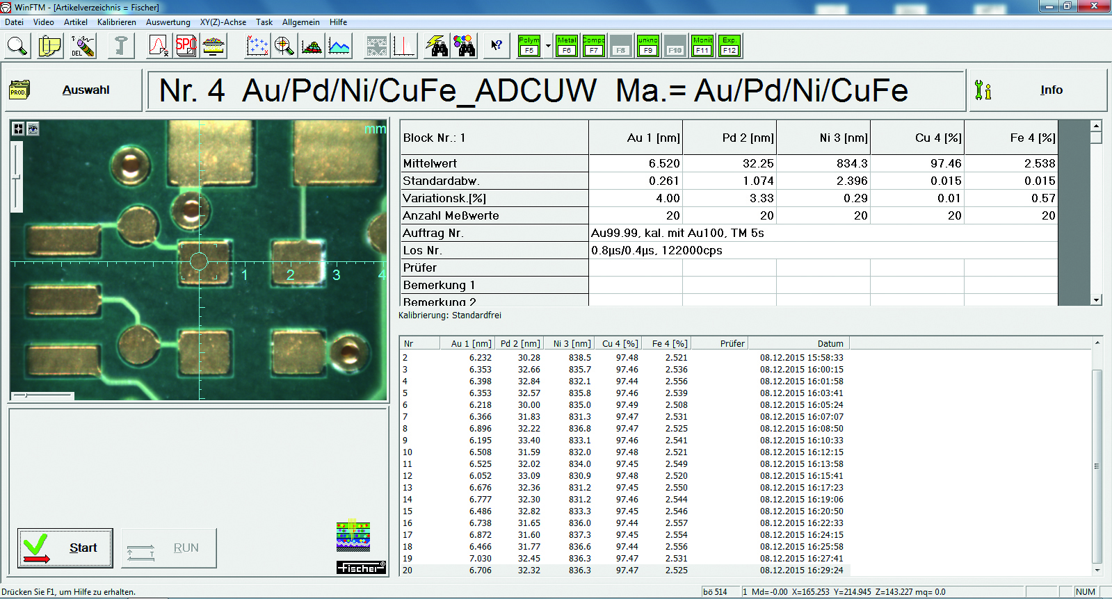
The non-invasive XRF is the most commonly used method to qualitatively and quantitatively ascertain a sample’s layers’ thickness in the nanometer and micrometer range.
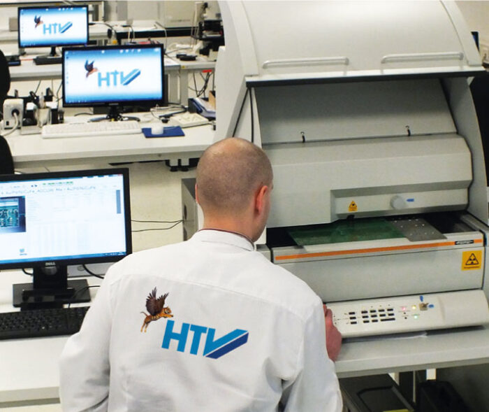
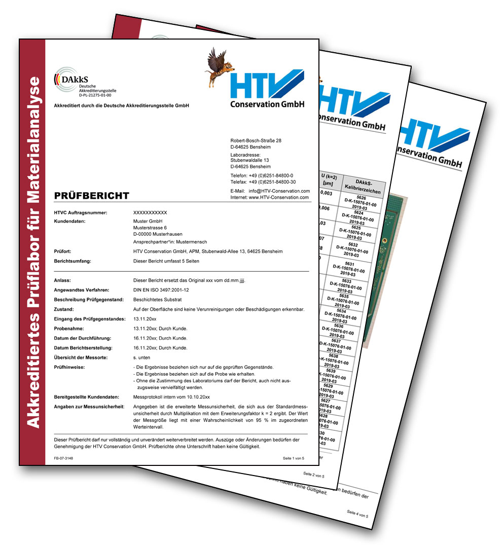
HTV’s accredited test laboratory for material analysis (international standard DIN EN ISO/IEC 17025) can perform layer thickness measurings of metals with the x-ray fluorescence method in accordance with DIN EN ISO 3497:2001-12.
For example, the hard gold platings on connectors or the layer thickness of a printed circuit board finish can be analyzed quickly and non-invasively, using the above mentioned method, both in regards to qualification and for serial quality control.
HTV: „ Incredible Performance “ at XRF – Proficiency test of the DRRR (german)
As one of a select few laboratories in Germany HTV can provide layer thickness measurements with the x-ray fluorescence method (XRF) which are internationally acknowledged and globally comparable.
Material analysis with the X-ray Fluorescence Method
Applied Standards
- ASTM B 568
- DIN EN 62321
- IPC-TM-650 Methode 2.3.44
Further analyses using the XRF method:
- Ascertaining an alloy’s composition
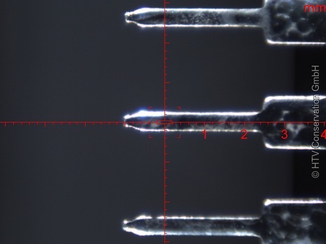
- Analyzing electronic components’ solder contacts’ composition (if they are lead free, for example)
- Identifying, i.e., ascertaining the elemental composition of unknown substances
- RoHS screening in regards to mercury, chrome, cadmium, lead and bromine (a full RoHS screening including PBBs, PBDEs and phthalates is also possible)
- Non-invasive measuring of raw circuit boards’ end surfaces
- Mapping to detect solder joints containing lead on assembled printed circuit boards
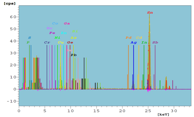
The non-invasive XRF makes it possible to identify or ascertain the fundamental composition of unknown substances, such as anorganic contamination on assemblies.
Given its low limit of detection, the XRF can in many cases also be used to screen in regards to RoHS restricted substances. For example, the solder contacts of components can be analyzed whether the are lead free or if they are coated correctly as part of an incoming goods inspection.
Alloy analyses, such as jewellery, as well as analyzing plastic materials in regards to halogenated or phosphorous flame inhibitors are further areas where the x-ray fluorescence analysis may be applied.
How the XRF differs from the energy dispersive x-ray analysis (EDX) under the scanning electron microscope (SEM)
- XRF uses an x-ray tube instead of an electron beam. Besides much more profound insights into the designated analysis area, this makes it possible to analyze moist or even liquid samples, as this method does not require a vacuum.
- Sample preparation is made significantly easer, as the sample does not need to be electrically conductive, meaning isolators like FR4 printed circuit boards or ceramics may be analyzed without any additional effort.