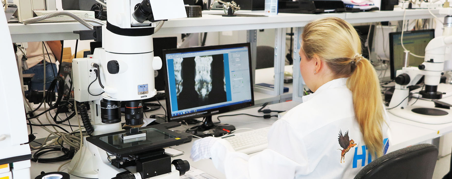
Light microscopy as an analysis and documentation method
Areas of application:
- Analyzing printed circuit boards and assemblies
- Examining the surface of electronic components’ contact pins
- Fracture surface analysis
- Investigation in regards to occurrence of oxidation and diffusion effects
- Measuring layer thicknesses and layer structures
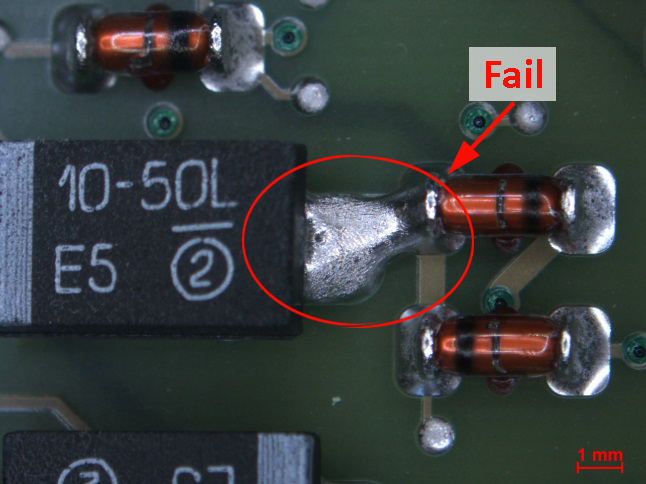
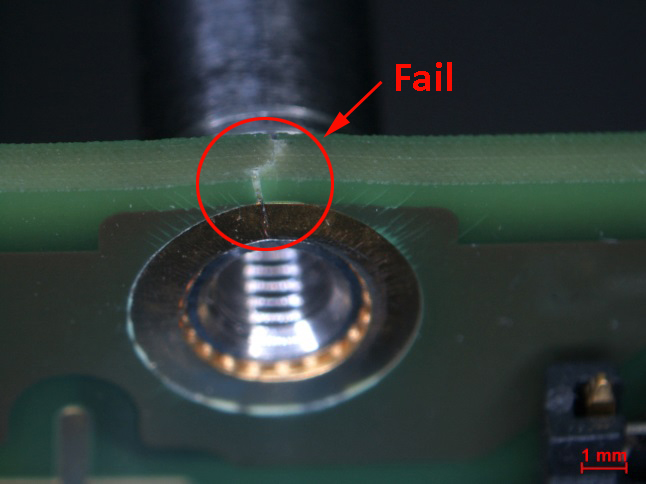
- Documenting deformations, damages and fractures on electronic components
- Examining of solder joint quality
In order to properly document damaged components as well examine solder joints or pre-prepared samples, i.e., microsections, light microscopy is an essential and important analysis method.
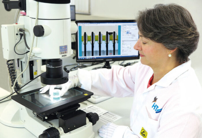
Depending on the problem and the size of the samples a variety of modern high-resolution microscopes with several configuration options are available to achieve optimum analysis results, e.g., reflected and transmitted light as well as dark field inspection methods.
Images are digitized by use of high-resolution cameras and are standardly provided in a complete examination report. Due to special image processing tools identified problem areas can be clearly highlighted and marked.
The light microscopy is an essential method, for example, to inspect printed circuit boards in accordance with IPC-A-610.
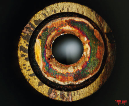
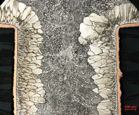
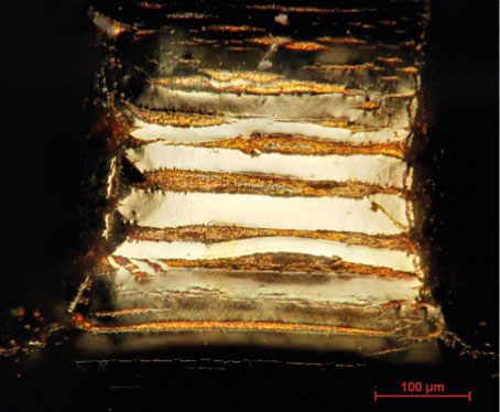
Examples of damaged electronic components